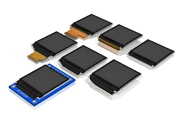
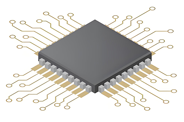
This resource provides in-depth information on the most advanced SPICE models for thin-film transistor (TFT) devices, essential components in modern lcd panel technology. These models enable accurate simulation and analysis of TFT behavior, critical for optimizing performance in various display applications. From conventional MOSFETs to cutting-edge oxide semiconductor devices, our comprehensive coverage supports engineers and researchers in developing next-generation display technologies.Optical Transceiver.
The following sections detail the modeling approaches for different TFT technologies, highlighting their specific characteristics, parameter extraction methods, and applications in lcd panel design and manufacturing. Each model is presented with its mathematical formulation, simulation results, and comparative analysis to facilitate practical implementation.
1. MOSFET Device Model
The Metal-Oxide-Semiconductor Field-Effect Transistor (MOSFET) serves as the foundation for most thin-film transistor technologies used in lcd panel applications. MOSFETs operate by controlling the flow of current between the source and drain terminals through an electric field generated by the gate electrode, separated from the channel by a thin insulating oxide layer.
The core SPICE models for MOSFETs, such as the Level 1 to Level 49 models in SPICE and BSIM (Berkeley Short-Channel IGFET Model) series, provide increasingly accurate representations of device behavior. These models account for various physical phenomena including channel length modulation, mobility degradation, velocity saturation, and leakage currents.
For lcd panel applications, MOSFET models must accurately predict threshold voltage, on-current, off-current, and switching characteristics under different operating conditions. The drain current in saturation region is typically modeled as:
ID = (μnCox/2)(W/L)(VGS - VT)²(1 + λVDS)
where μn is the electron mobility, Cox is the oxide capacitance per unit area, W/L is the width-to-length ratio, VGS is the gate-source voltage, VT is the threshold voltage, and λ is the channel length modulation parameter.
Modern MOSFET models for lcd panel integration include advanced effects such as short-channel effects, hot-carrier degradation, and temperature dependence, ensuring accurate simulation of circuit behavior across the entire operating range of display devices.
MOSFET Structure and I-V Characteristics
Key Model Parameters:
- VT - Threshold voltage
- KP - Transconductance parameter
- λ - Channel length modulation
- CGS, CGD, CGB - Gate capacitances
- φB - Bulk junction potential
- τOX - Oxide thickness
2. Hydrogenated Amorphous Silicon TFT Device Model
Hydrogenated amorphous silicon (a-Si:H) TFTs have been widely adopted in lcd panel technology due to their low cost, large-area fabrication capability, and compatibility with glass substrates. These devices differ significantly from crystalline MOSFETs due to the disordered nature of the amorphous silicon channel.
The SPICE models for a-Si:H TFTs must account for unique characteristics such as exponential dependence of mobility on gate voltage, stretched-exponential time dependence of threshold voltage, and significant leakage currents. The mobility in a-Si:H TFTs typically follows:
μ(VGS) = μ0 exp(γ√(VGS - VT))
where μ0 is the low-field mobility and γ is the mobility activation parameter. This mobility model significantly affects the transfer characteristics compared to crystalline MOSFETs.
For lcd panel applications, a-Si:H TFT models must accurately predict the device behavior under varying temperature and illumination conditions, as these environmental factors significantly impact display performance. The models typically include parameters for density of states in the bandgap, trap distributions, and recombination mechanisms.
Advanced a-Si:H TFT models incorporate self-heating effects and bias-stress induced threshold voltage shifts, critical for predicting long-term reliability of lcd panel operation. These models enable designers to optimize pixel circuits for maximum stability and minimum power consumption.
a-Si:H TFT Structure and Characteristics

Typical Properties:
- Mobility: 0.5-1 cm²/Vs
- On/off ratio: 10⁶-10⁷
- VT: 1-5 V
- Channel material: a-Si:H
LCD Panel Applications:
- TV displays (32"-75")
- Monitor panels
- Large format displays
- Automotive displays
3. LTPS TFT Device Model
Low-Temperature Poly-Silicon (LTPS) TFTs represent a significant advancement in lcd panel technology, offering higher electron mobility and improved performance compared to a-Si:H TFTs. Fabricated using laser annealing processes that convert amorphous silicon into polycrystalline silicon at temperatures compatible with glass substrates, LTPS TFTs enable higher resolution and more compact pixel designs.
The SPICE models for LTPS TFTs must account for the polycrystalline nature of the channel material, including grain boundaries, trap states at grain interfaces, and variations in crystallinity. These factors contribute to phenomena such as threshold voltage variability, kink effects, and anomalous leakage currents.
In lcd panel applications, LTPS TFT models require accurate representation of both n-channel and p-channel devices, as LTPS technology enables complementary circuits that reduce power consumption and improve noise immunity. The drain current model typically includes terms for:
- Grain boundary scattering effects on mobility
- Trap-limited conduction in the channel
- Band-to-band tunneling in the drain junction
- Self-heating effects in small-pixel applications
The higher mobility of LTPS TFTs (100-300 cm²/Vs) enables faster switching speeds, making them ideal for high-refresh-rate lcd panel applications and integration of driver circuits directly on the display substrate, reducing bezel size and system cost.
Advanced LTPS models incorporate bias temperature instability (BTI) and hot carrier injection (HCI) effects to predict long-term reliability, essential for automotive and industrial lcd panel applications requiring extended operational lifetimes.
LTPS TFT Performance Comparison
Key Advantages in LCD Panels:
4. IGZO TFT Device Model
Indium Gallium Zinc Oxide (IGZO) TFTs have emerged as a leading technology for high-performance lcd panel applications, offering the advantages of both a-Si:H and LTPS technologies. As an amorphous oxide semiconductor, IGZO provides high electron mobility (10-50 cm²/Vs) while maintaining the large-area uniformity and low-temperature processing benefits of amorphous materials.
The unique electronic structure of IGZO, with a conduction band derived from spherically symmetric s-orbitals of metal cations, results in high electron mobility even in the amorphous state. This characteristic enables IGZO TFTs to achieve superior performance compared to a-Si:H while maintaining better uniformity than LTPS across large lcd panel areas.
IGZO TFT SPICE models must account for several distinctive features:
ID = (μFECOXW)/(2L) × [ (VGS - VTH)VDS - (VDS²)/(2(1 + VDS/VSAT)) ]
where μFE is the field-effect mobility and VSAT is the saturation voltage. This model incorporates the unique velocity saturation behavior observed in oxide semiconductors.
For lcd panel applications, IGZO TFT models must accurately represent threshold voltage stability under prolonged bias and light illumination, as these factors significantly impact display performance over time. The models typically include parameters for oxygen vacancy defects, which play a critical role in determining device characteristics.
The combination of high mobility, good uniformity, and low leakage current makes IGZO TFTs particularly well-suited for high-resolution lcd panel applications, including 4K and 8K displays, where they enable smaller pixel sizes and lower power consumption compared to traditional a-Si:H technologies.
IGZO TFT Properties and Applications

| Parameter | IGZO TFT | a-Si:H TFT | LTPS TFT |
|---|---|---|---|
| Mobility (cm²/Vs) | 10-50 | 0.5-1 | 100-300 |
| On/off ratio | 10⁹-10¹⁰ | 10⁶-10⁷ | 10⁸-10⁹ |
| Uniformity | Excellent | Good | Fair |
| LCD Panel Cost | Medium | Low | High |
5. Thin-Film Transistor Stress and Aging Effects
Stress and aging effects in thin-film transistors significantly impact the long-term performance and reliability of lcd panel devices. These effects manifest as shifts in key device parameters, particularly threshold voltage (VT), which can lead to image sticking, brightness non-uniformity, and ultimately display failure if not properly accounted for in device models.Electronic shelf labels.
The primary stress mechanisms affecting TFTs in lcd panel applications include:
- Bias Temperature Stress (BTS): Threshold voltage shifts caused by prolonged application of gate voltage at elevated temperatures
- Light Illumination Stress: Photo-induced changes in device characteristics, particularly significant in a-Si:H TFTs
- Humidity Stress: Moisture-induced degradation of device performance, especially at the interfaces
- Mechanical Stress: Effects from thermal expansion mismatch and bending in flexible displays
The time dependence of threshold voltage shift under constant stress is often modeled using a stretched exponential function:
ΔVT(t) = ΔVT0 [1 - exp(-(t/τ)β)]
where ΔVT0 is the saturated threshold voltage shift, τ is the characteristic time constant, and β is the stretching exponent (0 < β < 1).
For lcd panel reliability modeling, these stress effects must be incorporated into SPICE models to predict long-term performance. Advanced models include temperature acceleration factors, enabling extrapolation of device lifetime from accelerated stress tests.Related Hydraulic Spare Parts
Understanding and modeling stress-induced degradation is critical for developing lcd panel technologies with extended lifetimes, particularly for automotive, avionic, and industrial applications where displays must operate reliably for 10+ years under harsh conditions. Compensation circuits based on these models can actively adjust for threshold voltage shifts, maintaining consistent display performance over the product lifetime. Related Lithium Battery Manufacturing.
TFT Aging Characteristics
Stress Mitigation Strategies in LCD Panels:
Material Engineering
Optimized gate insulators and passivation layers to reduce charge trapping
Circuit Design
Incorporation of feedback loops to compensate for threshold voltage shifts
Operating Condition Optimization
Reduced operating voltages and temperature management in lcd panel designs
TFT Technology Comparison for LCD Panel Applications
| Technology | Mobility (cm²/Vs) | On/Off Ratio | Uniformity | Cost | Best For |
|---|---|---|---|---|---|
| MOSFET | 500-1000 | 10¹² | Excellent | High | LCD driver ICs |
| a-Si:H TFT | 0.5-1 | 10⁶-10⁷ | Good | Low | Large lcd panel displays |
| LTPS TFT | 100-300 | 10⁸-10⁹ | Fair | High | High-res lcd panel with integrated drivers |
| IGZO TFT | 10-50 | 10⁹-10¹⁰ | Excellent | Medium | High-performance lcd panel displays |